STEP-MXO2 FPGA Development Board for Educational Learning
EIM technology has come up with STEP-MXO2 FPGA development board, a compact, breadboard-friendly, and easy-to-learn hardware design platform built around the Lattice MachXO2 FPGA. It is targeted mainly for educational purposes.
EIM technology has come up with STEP-MXO2 FPGA development board, a compact, breadboard-friendly, and easy-to-learn hardware design platform built around the Lattice MachXO2 FPGA. It is targeted mainly for educational purposes. Hence, it offers several features that allow users to implement a wide range of designed circuits, from simple circuits to various creative applications.
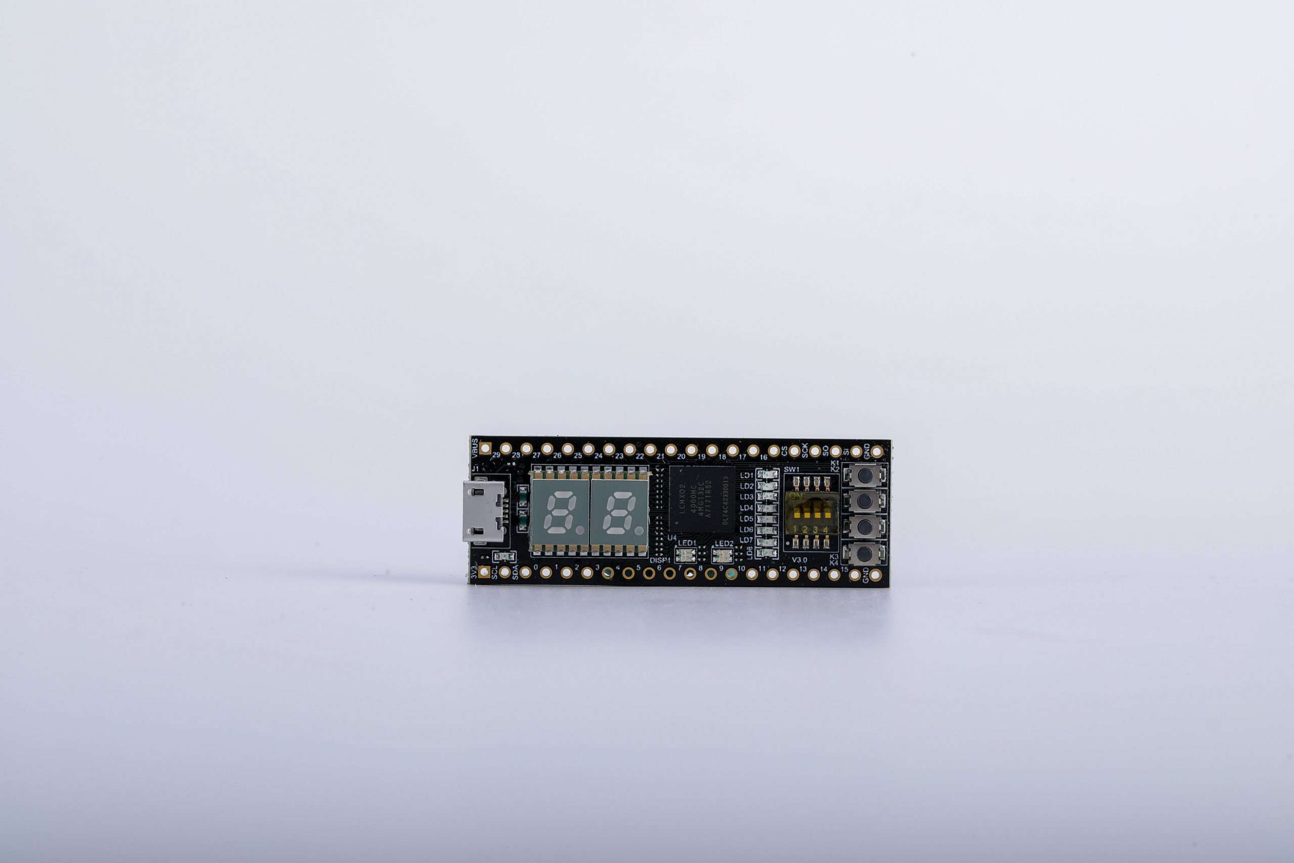
STEP-MXO2 FPGA is a compact 40-pin DIP FPGA development board. The board is both robust and portable, and it needs a power supply of 5V DC input through a Micro-USB connector. The hardware features an onboard JTAG Programmer, clock source, 7-Segment Displays, LEDs, GPIOs, and much more. Because of these components, it is a formidable platform for designing digital logic circuits and Micro32 embedded soft-core processors using Lattice Diamond software. Hence, STEP-MXO2 becomes the ideal option for learning FPGA, evaluating, and prototyping the true potential of the MXO2 FPGA by using all of these features.
Technical Specifications of STEP-MXO2 FPGA
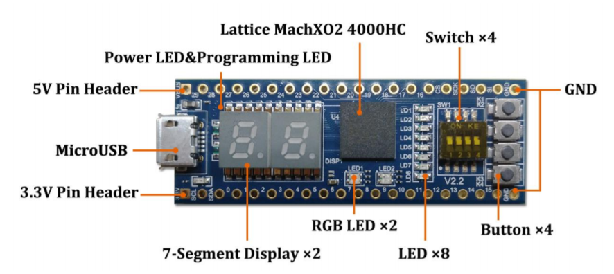
- Lattice MachXO2 FPGA: LCMXO2-4000HE-4MG132
- On-Board JTAG Programming circuit (Normal Micro-USB connector)
- 2-character 7-segment display
- Two RGB LEDs
- Four switches
- Four push buttons
- Eight user LEDs
- Power from MicroUSB connector
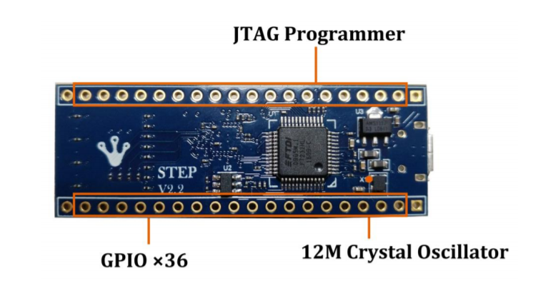
- 40 pins DIP connector with 36 User I/Os
Additionally, the onboard MachXO2-4000HC FPGA provides embedded Flash technology for instanton, non-volatile operation on a single chip. All connections are through the MachXO2 chip to provide maximum flexibility for the user. This allows the user to customize the FPGA to implement any system design. Numerous system functions are also included, such as two PLLs and 10 Kbits of embedded RAM plus hardened implementations of I2C, and user Flash memory.
You can integrate your programmable design directly into solderless breadboards by routing 36 digital FPGA I/O signals to 100-mil-spaced through-hole pins. These 36 user I/Os comprise 30 GPIOs, four dual-functional pins default to SPI interface, and two dual-functional pins default to I2C interface. It also loads into a standard socket for using it in embedded systems. Thanks to its small size of 0.72 inches by 2.05 inches.
The motive of creating STEP-MXO2 according to Tindie:
“It is difficult to learn FPGA, not only because the content and material are complex to understand, but also access to the hardware is challenging. However,it aims at an educational purpose for entering level to learn FPGA.”
Software Support
Coming to the software part, the STEP-MX02 Dev board is based on Lattice Diamond design software. This software provides leading-edge design and implementation tools optimized for low-power, cost-sensitive Lattice FPGA architectures. Additionally, the software accelerates the development of Lattice FPGA-based applications for a variety of sectors, including industrial/automotive, communications/computing, and consumer.
The STEP-MX02 Dev board is available on Tindie at $54.99. The board comes with learning materials suitable for FPGA learners, including a QuickStart guide, user manual, schematic documentation, and demos. For those just starting out, introductory FPGA training courses are also available.
For more information visit the official product page. Images and technical specifications have also been taken from the product page.


