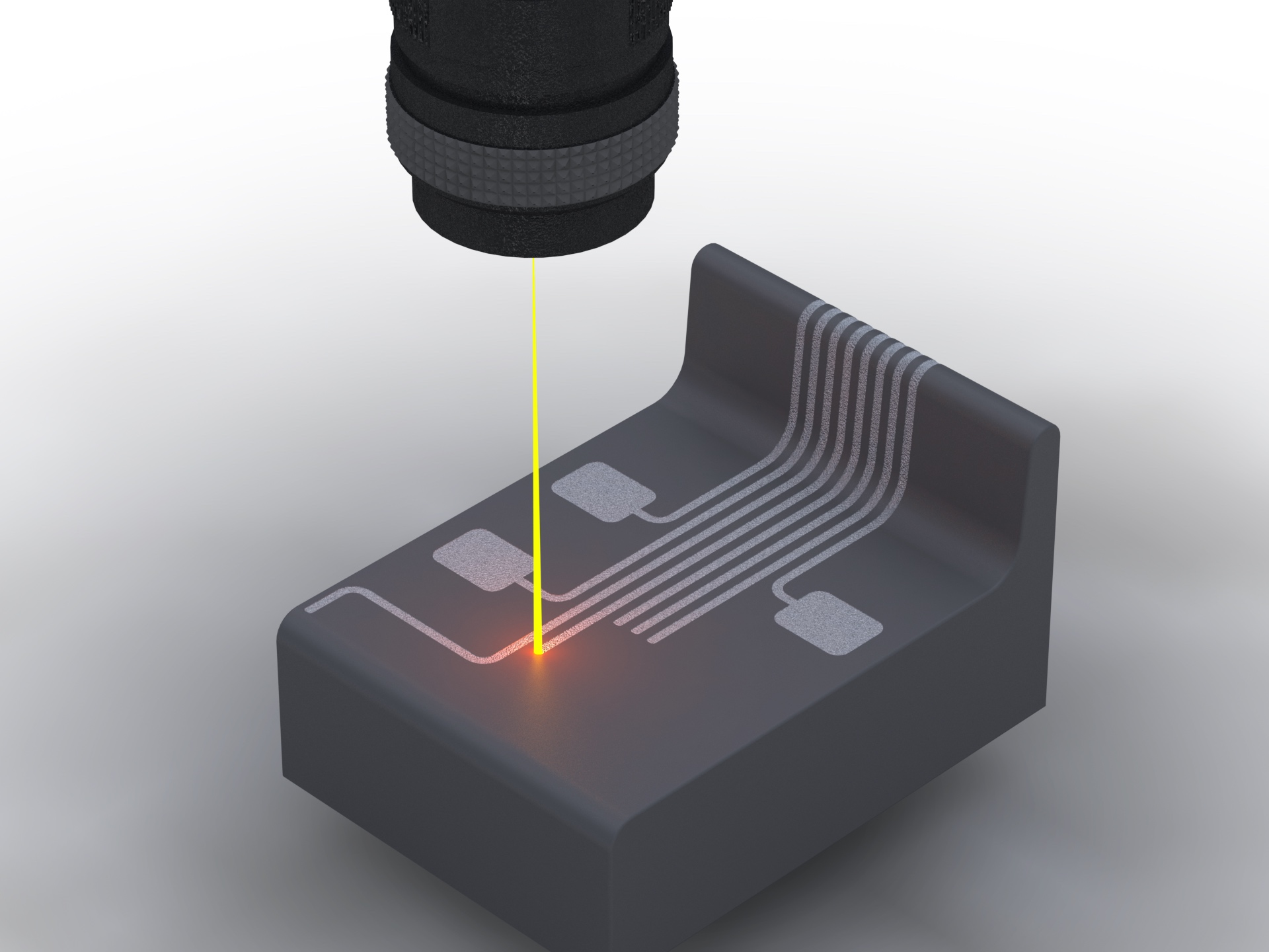
Laser direct structuring (LDS) is a special success story. For almost 20 years, it has been possible to apply electronic conductor paths directly onto plastic parts during series production. Laser Direct Structuring (LDS) – The structure of the conductor path is applied using the LDS process.
LDS enables electronic assemblies to be made in flexible geometric shapes. Smart phones, hearing aids and smart watches are becoming smaller and more powerful thanks to this process.
LDS enables the production of electronic assemblies with flexible geometric shapes. This process enables electronic products (such as smart phones, sensors or medical devices) to become even smaller and more powerful. Automated manufacturing processes also make this process more economically attractive.
There is less and less space available for electronic assemblies, so solutions are needed which replace conventional printed circuit boards. LDS enables further miniaturisation and makes increasingly complex geometric designs possible. This is a stable and reliable process that has established itself in quality-critical sectors such as medical technology or safety-relevant components for the automotive industry.
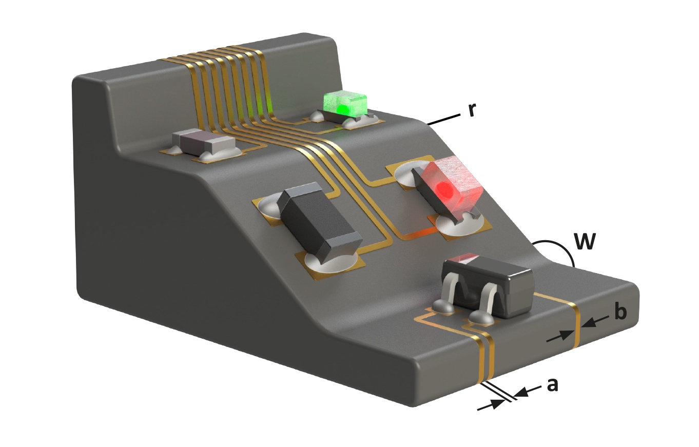
The LDS process enables three-dimensional assemblies Direct laser structuring enables 3D-MID (Mechatronic Integrated Devices) assemblies to be produced. When using 3D-MID, electronic components can be fitted directly onto a three-dimensional base body, without circuit boards or connecting cables. The base body is manufactured using an injection moulding process, whereby the thermoplastic material has a non-conductive, inorganic additive.
New trends in the LDS process
Several aspects of LDS technology have been improved and further developed over the past few years.
The working area of the laser has been enlarged from 160 x 160 x 80 mm to 200 mm x 200 mm x 80 mm, thus enabling a higher packing density and the processing of even larger components. The working speed of the laser can be doubled to 4 m/s by optimising the servo units and mirrors which guide the laser beam, thereby significantly reducing the processing time. The improvement of the optics enables the use of a laser with a diameter of 100 μm and a laser with a fine focus of 50 μm for processing even smaller structures.HARTING is the only 3D-MID manufacturer in the world that has a laser system with three fine focus optics of 50 μm. Even smaller conductor path gaps can be achieved thanks to this fine focus laser. Thus, many conductor paths can be created on the same component and a higher packing density can be implemented. This is used for safety technology, among other things, because the closely spaced and intertwined conductors are capable of triggering safety alarms from even the smallest physical interference.
Advances in materials and economics
Only specially selected thermoplastics are certified for the LDS process; these are available from stock. The process can be further improved with customer-specific adjustments to the plastic material:
HARTING uses a process which adds LDS additives to non-certified materials to make them MID-compatible. Specific RAL or Pantone colours can be achieved with MID plastics by using colour pigments and special LDS additives. By selecting suitable additives, special RF characteristics can also be implemented, depending on the frequency range.
Component carrier – Electronic components – such as LEDs, ICs, photodiodes and sensors – can be attached directly onto the component carrier. The assembled component carriers can then be processed as standard SMD components.
To further improve the cost-effectiveness of the manufacturing process, HARTING relies on automated robotic systems. The LDS laser system is equipped with a rotary indexing table so that a component can be inserted or removed while another component is still being processed. The in-feed and unloading procedures are automated by HARTING using robotics. This increases throughput and autonomy, while also enabling integration into automated production processes. An additional automation step is provided during the injection moulding process. Here, too, a robot takes over the removal of the injection moulded parts. The use of robotics also improves the precise reproducibility of the processes and, thus, overall product quality.
More growth for 3D-MID
Security caps for payment terminals – The 3D-MID caps protect the electronics from unauthorized access both mechanically and electronically. A highly precise meandering structure detects every access, no matter how small, and consequently prevents theft.
HARTING reports increased demand for MID projects and has further expanded the 3D-MID division by investing in machinery and by acquiring a competitor’s business. Innovative in-house products are also contributing to further growth. HARTING has developed a solution based on 3D-MID technology which replaces flexible PCBs with a component carrier. Instead of using a flex-PCB, the component carrier can be fitted directly with electronic components, thus saving up to two thirds of the cost.
About HARTING 3D-MID: www.HARTING.com/3D-MID


OK, this post is in the top 10 coolest posts I’ve read here. Thanks.