Juergen’s 100 MHz 65F02 Microprocessor is designed to work as an Accelerator for 6502 And 65C02 Computers
The 8-bit, 2 MHz 6502 microprocessor of MOS Technology, now CSG, had gained widespread use on classic computers of the late 1970s and early 1990s, like the Apple II plus, games consoles, and chess computers, though the games consoles and chess computers were mostly CMOS 65C02-based. The CMOS-enhanced 65C02 version of the microprocessor which is still available today under the ownership of Western Design Centre, Inc (WDC) now appears to be overtaken as there is now a new microprocessor that beats its clock cycle by a great magnitude of 86MHz (against 14 MHz clock cycle).
The 8-bit, 2 MHz 6502 microprocessor of MOS Technology, now CSG, had gained widespread use on classic computers of the late 1970s and early 1990s, like the Apple II plus, games consoles, and chess computers, though the games consoles and chess computers were mostly CMOS 65C02-based. The CMOS-enhanced 65C02 version of the microprocessor which is still available today under the ownership of Western Design Centre, Inc (WDC) now appears to be overtaken as there is now a new microprocessor that beats its clock cycle by a great magnitude of 86MHz (against 14 MHz clock cycle).
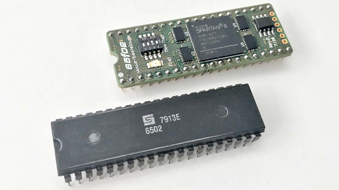
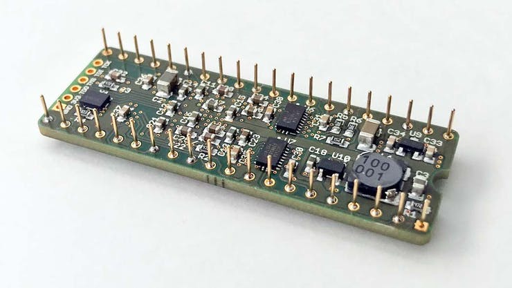
The newest project from Juergen is a 6502/65C02 CPU core in an FPGA designed to upgrade and run vintage computers and games at 100 MHz. The 65F02 is a Spartan-6 FPGA with a 64 KByte on-chip RAM fixed on a 40-pin dual inline PCB with the same pinout as 6502 and 65C02 CPU. The FPGA consists of a logic that can read the external 6502 bus with accurate timing depending on the clock that comes in from the host device. The PCB view of the 65F02’s topside shows the Spartan-6 FPGA, LED, configurable switches, and flash memory. The bottom side debuts voltage regulator, clock oscillator, decoupling capacitors, level converters for 5V input signals, and 40-pins interface. Its PCB can fit directly into a 40-pin DIP socket designed for 40-pin IC.
The 65F02 is designed to work as a standalone universal accelerator for 6505/65C02 once it replaces the original CPU and fits on the CPU socket. Once it is fixed, the FPGA board identifies the host’s memory map and takes over the entire RAM and ROM content, and copies it into the onboard RAM (except for the I/O area) upon power-on. The CPU keeps running with the internal memory at 100 Mhz for all bus accesses except for I/O addresses for which it pauses for an external bus cycle to commence depending on the external clock speed. According to the designer, prototypes of 65F02 have been successfully tested in an Apple II, Commodore 8032, and chess computers like Mephisto Milano with this method of integrating an accelerator into a host. He added that the board is yet a hobby project and there is no plan to go into commercial production at the moment.
According to him, limitations and incompatibilities associated with the board include the need for memory expansion board and back switching to be known to the 65F02 since its onboard 64 KByte is not sufficient for it to fully accelerate the extended memory where large memory is involved. Also, there is a problem of incompatible software or add-on hardware as a result of time-lapse created while the 65F02 tries to read access to time-critical external devices and switch back to the original slow speed temporarily.
Furthermore, vintage computing – 65F02 has all design files and documentation available. For the main circuit board and USB programming adapter designs, there are AutoCAD Eagle Format (version 7 . x) files to assist in reproduction. Also, there is an FPGA source file for Xilinx WebISE 14.7 if you need to modify the FPGA source file.
For more information, support and documentation, open-source components, visit Juergen@e-basteln.de


This article is four years old. Are there any updates on progress?