


Researches Solve Problems of Organic Thin Film Transistors By Developing Nanostructured Gate Dielectric
Amorphous silicon-based Thin-film transistors (TFTs) are the foundation of many modern-day technologies, such as smartphones and flat-panel TVs. Still, it comes with a few drawbacks like performance limitations due to limited carrier mobility. Provoking the researchers in search of something better.
As a result, Organic thin-film transistors (OTFTs) were developed. OTFTs have solved the problem with carrier mobility to an extent. Although it introduced new problems such as the critical performance parameter of large threshold voltage instabilities. Threshold voltages—also known as gate voltages—are the minimum voltage differential needed between a gate and the source to create a conducting path between the source and drain terminals.
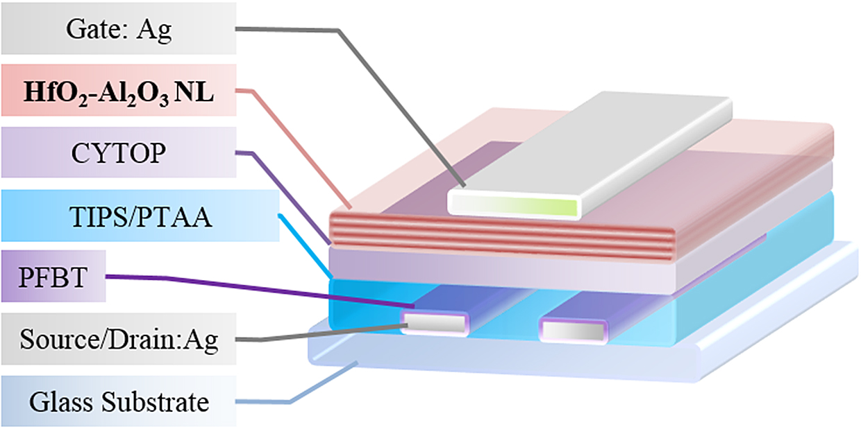
Latest works of the researchers at Georgia Institute of Technology seems to overcome the voltage instability problem with OTFTs. They have developed a nanostructured gate dielectric that can regulate voltage threshold fluctuations in OTFTs.
A gate dielectric is an important component of every thin-film transistor. It acts as the electrically insulating layer between the gate terminal and the semiconductor. It should have a high dielectric constant, be very thin, and have a high dielectric strength for the transistor to function at low voltage.
On applying a voltage across the gate electrode, the resulting electric field across this insulating layer changes the density of carriers in the semiconductor layer. It regulates the current that is flowing between the source and the drain electrodes. Many different materials are used to make this insulating layer. Such as dielectric polymers, inorganic oxides or combinations of different organic and inorganic materials.
The Georgia Tech researchers used Atomic Layer Deposition (ALD) technique to build a thin metal oxide layer on top of a perfluorinated dielectric polymer. They chose ALD for its ability to produce layers that are free from any defects. Bernard Kippelen, a professor at Georgia Tech, and leader of the research said:
The low defect density reduces the diffusion of moisture into the underlying organic semiconductor layer, preventing its degradation.
The performance of the new organic thin-film transistors seems to surpass that of hydrogenated amorphous silicon technology. According to Kippelen, it revolutionizes OTFTs in terms of charge mobility and stability. He stated:
It is premature and difficult at this stage to provide a direct comparison with what is currently on the market; nevertheless, we believe that the level of stability that is achieved is an important step for printed electronics.
Before the future applications, Kippelen and his team will further investigate the mechanical properties of these printed transistors since they show great potential with flexible form factor products. Further information can be found on the Research paper published in the journal Science Advances.
RELATED POSTS
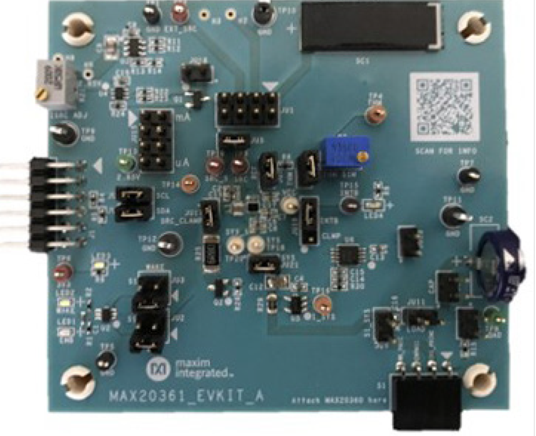 4 February, 2021 MAX20361 Tiny Single-/Multi-Cell Solar Harvester works from 225mV
 28 November, 2016 Introducing Autodesk Circuits Simulator For Beginner
 5 December, 2018 3.6A Bidirectional DC Motor Driver Shield for Arduino Nano
 28 August, 2020 Avalue introduces the Latest Embedded Products with Intel® Apollo Lake Processor ECS-APCL, an Intel Celeron J3455 Fanless System
 17 July, 2019 AOPEN DE5500 – SFF PC features 7th generation Intel® Core
 19 May, 2021 Analog Devices LT8491 Buck-Boost Battery Charge Controller


