


U.S. Department of Energy’s Lawrence Berkeley National Laboratory (Berkeley Lab) has developed a way to assemble transistors based on the 2D materials graphene and molybdenum disulfide. By Peter Clarke @ edn-europe.com
The method etches narrow channels in conducting graphene laid down on a silicon-dioxide substrate. These channels are then filled with a transition-metal dichalcogenide, or TMDC, or more specifically MoS2. Both of these materials have a 2D structure that is just one atomic layer thick. The synthesis method was able to cover an area a few centimeters long by a few a millimeters wide opening up the possibility of commercial-scale production in a wafer fab on a silicon wafer.
Berkeley Lab makes graphene-MoS2 transistor – [Link]
Please follow and like us:
RELATED POSTS
 26 November, 2015 Raspberry Pi Zero: the $5 computer
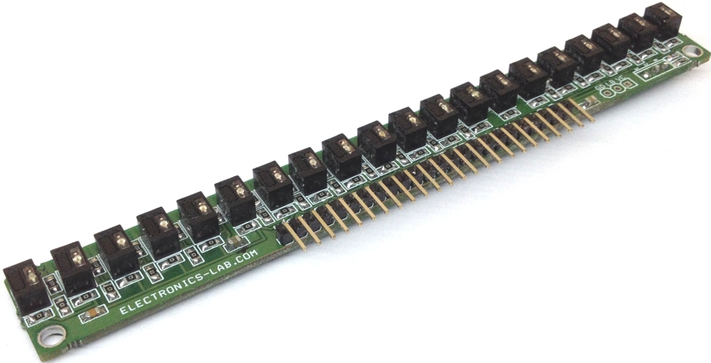 30 April, 2020 20 Non-Contact Infrared Reflective Sensor for Line Follower Robots
 29 June, 2016 Contactless OLED Thermometer With Arduino and MLX90614
 18 November, 2015 HacKeyboard – open hardware mechanical keyboard
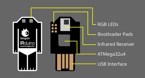 1 December, 2017 IRduino – Arduino-compatible USB infrared receiver
 5 June, 2016 DIY Voltmeter using a simple voltage sensor and Arduino Uno and a Nokia 5110 LCD
Subscribe
Login
0 Comments