Introducing NRFICE: A Bluetooth FPGA Board for Edge Computing and IoT Applications
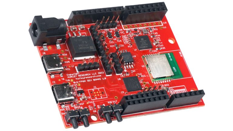
The NRFICE is a Bluetooth FPGA board designed to be compatible with the Arduino UNO form factor. It combines two key components: the dual-core nRF5340 Bluetooth SoC and the LatticeICE40UP5K FPGA.
The NRFICE is a Bluetooth FPGA board designed to be compatible with the Arduino UNO form factor. It combines two key components: the dual-core nRF5340 Bluetooth SoC and the LatticeICE40UP5K FPGA.
The Lattice ICE40UP5K FPGA is known for its low power consumption and high performance, making it suitable for edge computing and artificial intelligence projects. On the other hand, the nRF5340 Bluetooth SoC is a versatile chip that supports various communication protocols such as Bluetooth Low Energy (BLE), Bluetooth Mesh, Thread, NFC, and Zigbee.
What sets NRFICE apart is its ability to directly load a project into the ICE40 FPGA through the nRF5340 chip. This eliminates the need for complex toolchain setups typically required for FPGA development. As a result, NRFICE enables a new approach to FPGA development, where users can host bitstreams in the cloud, select them using a mobile device, and wirelessly load them onto the board.
This innovative feature opens up possibilities for seamless and flexible FPGA development, allowing users to focus more on their projects and less on setup and configuration tasks.
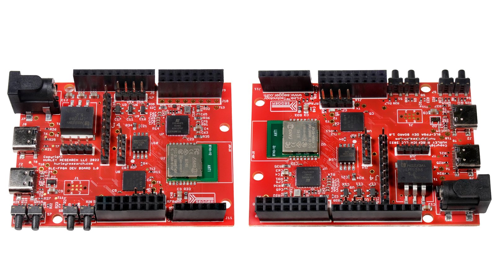
The NRFICE Bluetooth FPGA board comes with a built-in J-Link OB for easy debugging and programming, eliminating the need for emulator dongles. It supports Arduino Uno 3.3V shields and has a 5V power supply onboard, allowing it to power shields and daughterboards for various applications like LED lighting and motor control.
Key Specifications:
- Microcontroller: Nordic Semiconductor nRF5340, dual-core Bluetooth 5.3 SoC with 128MHz Cortex-M33, 1MB Flash, and 512KB RAM.
- FPGA: Lattice Semi ICE40UP5K with 5280 LUTs, 1024KB single-port RAM, and 120KB embedded block RAM.
- Network Capabilities: Bluetooth Low Energy, Bluetooth 5.3, LE Audio, direction finding, Bluetooth mesh, Thread, Zigbee, 802.15.4, and more.
- Buttons and LEDs: Reset buttons for ICE40 and nRF, user-programmable buttons, and RGB LEDs for status indication.
- USB Connectivity: USB-C for J-Link OB and nRF5340, providing VCOM serial port and other USB implementations.
- Power Supply: 9V – 12V via a barrel power connector, 5V @ 3A regulator.
- Form Factor: Arduino Uno is compatible with a 0.1” pinout.
NRFICE is an open-source project certified by OSHWA, offering access to its Bill of Materials, schematics, Gerber files, Verilog projects, and more on GitHub. It works with an open-source Android app for wireless programming and configuration of the nRF5340 chip and ICE40 FPGA. Additionally, professional development tools like Segger Embedded Studio and Lattice’s Radiant are available for free.
The NRFICE FPGA board is priced at $159 with free shipping within the US and a $12 shipping fee worldwide. The campaign on Crowd Supply has surpassed its funding goal, and orders are expected to ship by August 2, 2024.


