Next DFM: A PCBs Life-Saver?
Have you ever had problems with your PCB designs and had to remake any of them after having the "final" prototype in your hand? If you are one of these non-human geniuses that made only masterpiece-like, immaculate PCBs, please, throw the first stone.
Have you ever had problems with your PCB designs and had to remake any of them after having the “final” prototype in your hand? If you are one of these non-human geniuses that made only masterpiece-like, immaculate PCBs, please, throw the first stone. As we are not, and had to perform many revisions of our PCBs, we are always looking for ways to minimize our (expected) human errors, which can save us some money at the end of the day. This is why we bring today to the table, to meet a possible new PCB design partner, Next DFM. Now, is it useful for you? Let us check on that.
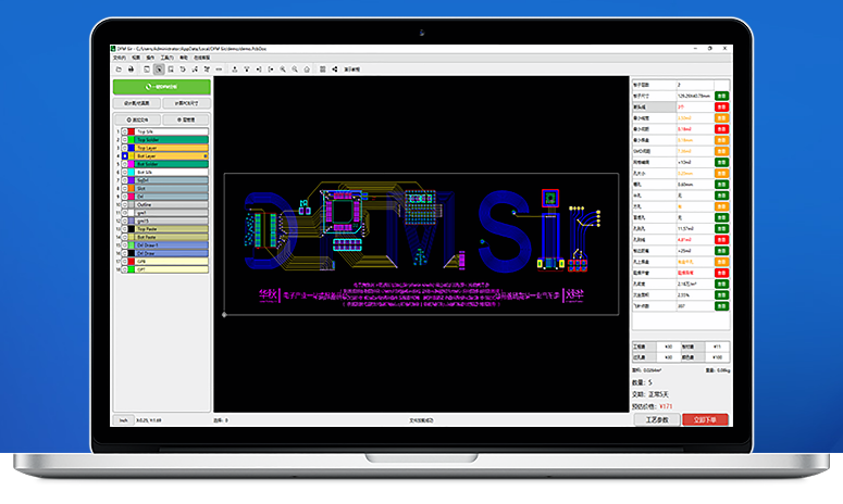
What is Next DFM? It is a PCB design analysis software, developed by the PCB boards manufacturer Next PCB. Being frustrated with many failed designs that end in the garbage pile, we decided to give this app a try. By placing the Gerber files on the Next DFM and running the DFM (Design For Manufacturability) analysis, the software gives you a considerable amount of information. Some of it is obvious to the designer (like the layer count and the dimensions), others may be interesting, such as minimum pad size, hole diameter, SMD’s spacing, minimum track width and spacing, hole to hole, and hole to track spacing, to name a few. But if you are a good designer, and using good software, as Altium example, most of the information given you already have configured on the rules before starting to route everything up, and checked it all after performing DRC (Design Rules Check).
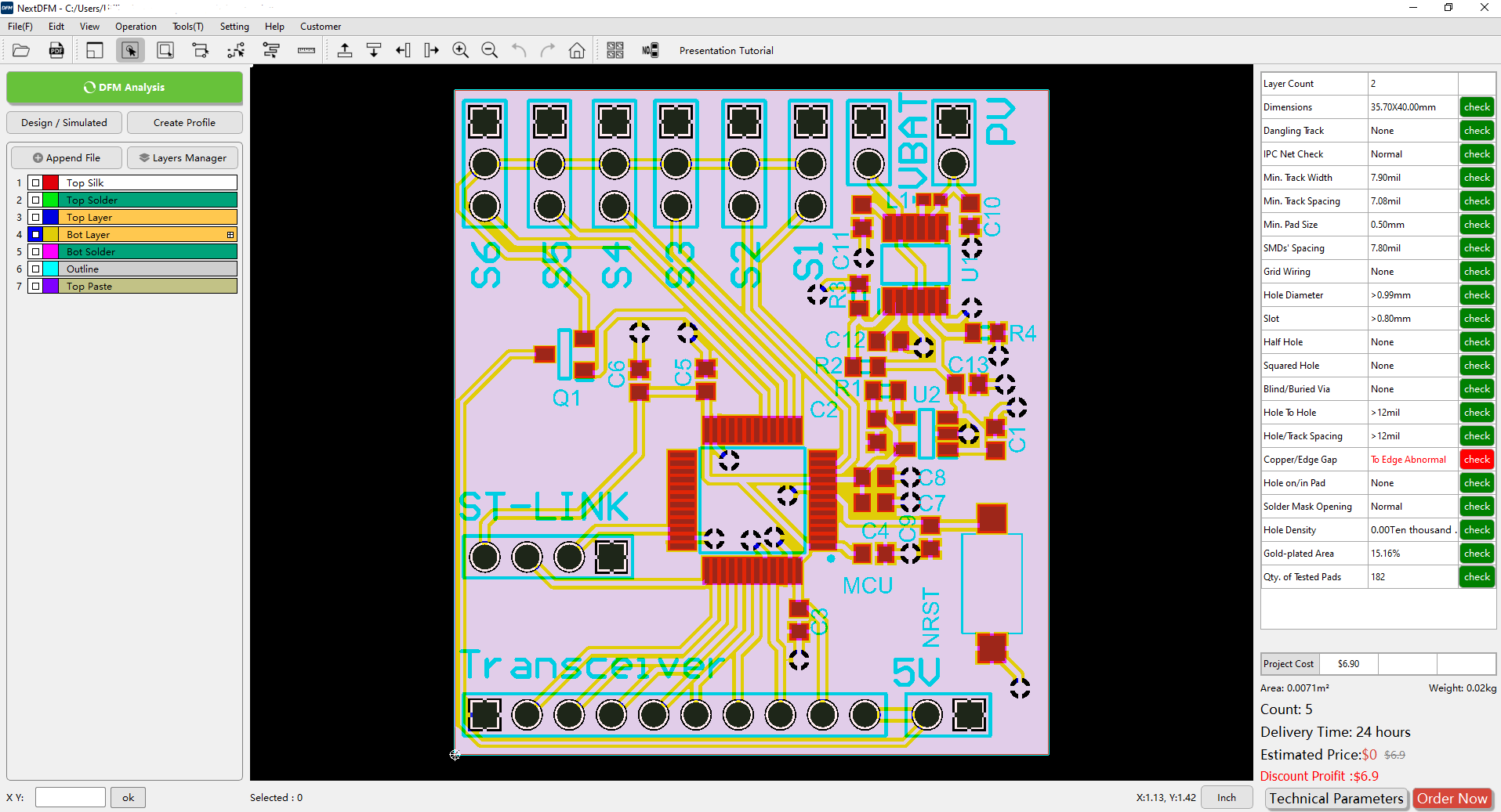
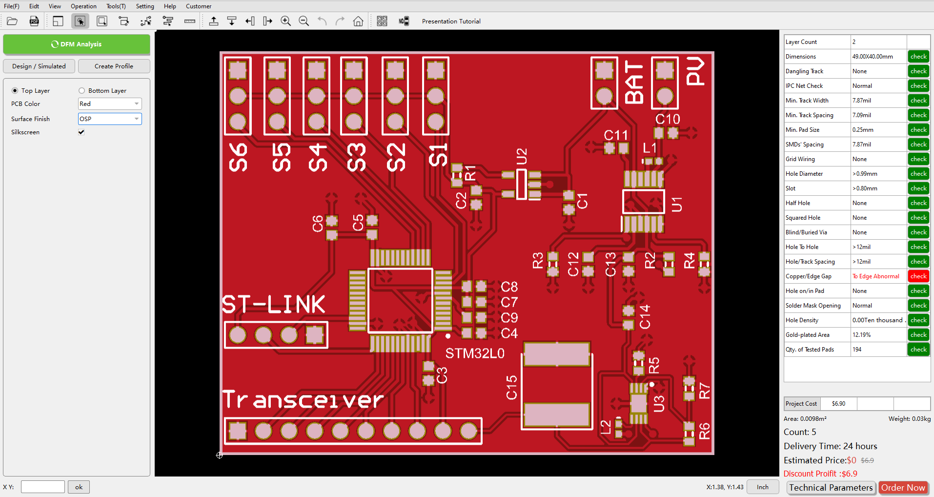
Along with the one-click analysis, which we have just seen, there are other two major functionalities in this app. Starting with the PCB physical simulation preview, it sort of works as the preliminary step in order to order a board, where you can easily switch the PCB color and its finish, check also the layers, and easily switch between the design and the simulation views.
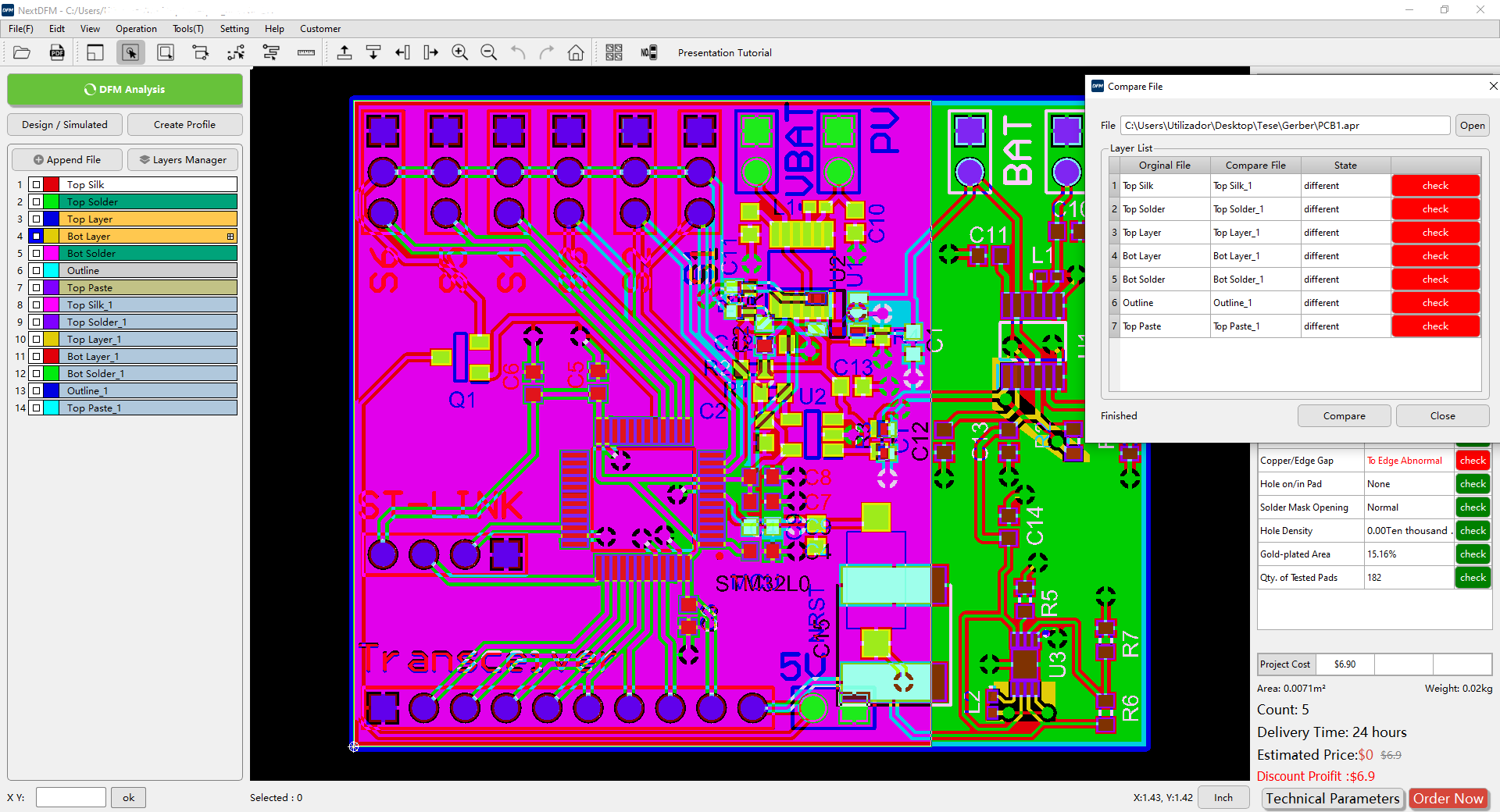
The last interesting function the Next DFM provides is the automative tool, which there may be some interesting hidden features. By clicking on the tools tab, you can calculate the impedance, compare files to check if they are the same and place them over one another (can come in handy when making changes to PCBs, so that you do not forget anything), perform panelization, calculate routing distance, utilization rate, soldering pads on each layer and check for open and short circuits, for which you will need the .ipc file.
To whom is the Next DFM available for? Firstly, Windows users. For now, the app is free, and it looks like it will be that way forever. The app is said to support files from Altium, Pads, and Protel99SE, but Gerbers are pretty much universal, so you can probably throw Eagle and KiCad EDA files to it and it probably will work too. Even though it is tightly coupled to the Next PCB brand, using buttons that link to order the PCB on their website and estimated order pricing, and simplifies the ordering process, avoiding those “we need said files to manufacture your PCB” emails. It begs the question: is it for you, if they are not your go-to PCB manufacturer? Well, you can give it a chance, see if it has more to offer than your favored PCB software. It is a relatively easy app on the computer, so you have got nothing to lose. My only complaint will be not having a tutorial for it, which can help many more users get into it.
Next DFM link: https://www.nextpcb.com/nextdfm.html