Pico-Ice Features Raspberry Pi RP2040 with a Lattice iCE40 FPGA
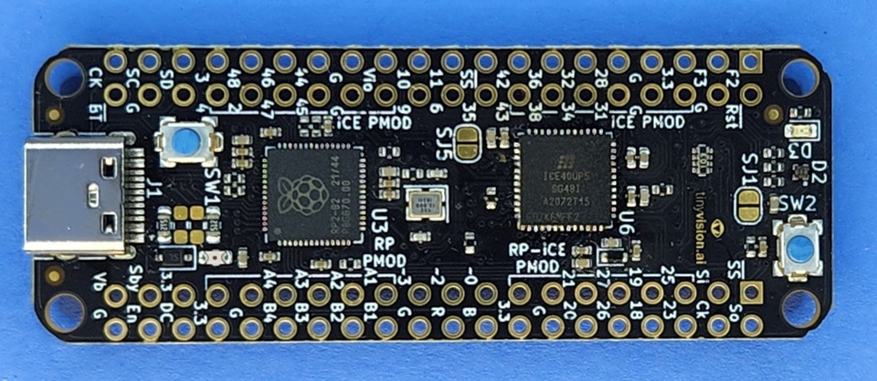
tinyVision.ai has introduced the "pico-ice," a compact gum stick-style development board that combines the power of a Raspberry Pi RP2040 dual-core microcontroller and a Lattice UltraPlus iCE40UP5K FPGA. The board is designed to be affordable and small, featuring independent flash for both the FPGA and RP2040, low-power SSRAM, a user-addressable RGB LED, and a couple of push buttons.
tinyVision.ai has introduced the “pico-ice,” a compact gum stick-style development board that combines the power of a Raspberry Pi RP2040 dual-core microcontroller and a Lattice UltraPlus iCE40UP5K FPGA. The board is designed to be affordable and small, featuring independent flash for both the FPGA and RP2040, low-power SSRAM, a user-addressable RGB LED, and a couple of push buttons. Moreover, the pico-ice offers an impressive array of GPIO pins brought out to easily accessible 0.1″ header pins (arranged as PMODs) for rapid prototyping.
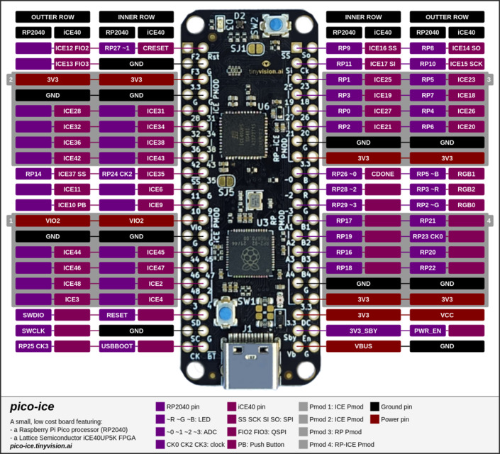
The Raspberry Pi RP2040 serves as the main controller on the board, equipped with a dual-core Arm Cortex-M0+ microcontroller running at a stock speed of 133MHz and 264kB of SRAM. Additionally, the RP2040 features a clever programmable input/output (PIO) system, enabling the definition of new hardware capabilities as state machines.
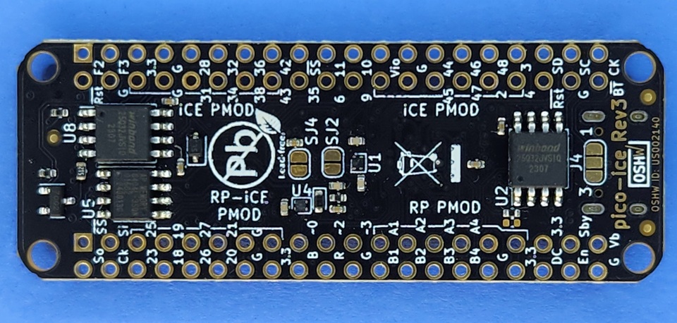
The board also includes the Lattice iCE40UP5K with 5.3k look-up tables (LUTs), 1Mb of single-port synchronous static RAM (SPRAM), 120kB of double-port RAM (DPRAM), and eight multipliers. There are 4MB of NOR flash connected via quad-SPI for each component, along with an additional 8MB of low-power SSRAM, which connects to the FPGA via QSPI and the RP2040 via SPI.
The generous GPIO capabilities are made accessible through twin 2×20-pin headers on either side of the board, with most of the pin-out divided into PMOD connectors. There is one dual PMOD for the microcontroller and two dual PMODs for the FPGA, along with another dual PMOD shared between the two.
For ease of use, the pico-ice is available for purchase as fully-assembled versions with bundled dual PMOD headers (which require fitting) through Lectronz, priced at $35. Furthermore, tinyVision.ai has released the design on GitHub under the permissive MIT license, making it open hardware.
Board and Firmware features:
- FPGA clock supplied by the RP2040, an easy-to-program FPGA clock under the control of the RP2040
- RP2040 can program the FPGA directly or the dedicated FPGA flash. Programming is done using a drag-drop of a UF2 file or using a command line DFU-based approach for flexibility.
- Sample RP2040 code provides a pass-through UART function for the FPGA
- An 8-bit wide bus between FPGA and RP2040 can be used for qSPI, UART, etc.
- Support for ultra-low power sleep mode: can shut down the RP2040 and FPGA while keeping the SRAM powered (tens of uA in standby)
It’s worth noting that the creation of this board was a collaborative community effort, with multiple individuals contributing to both the board’s design and firmware development.
For more information about the pico-ice, visit the product page. For documentation, visit the GitHub page.


