Current Loop Sensor Using GreenPAK™
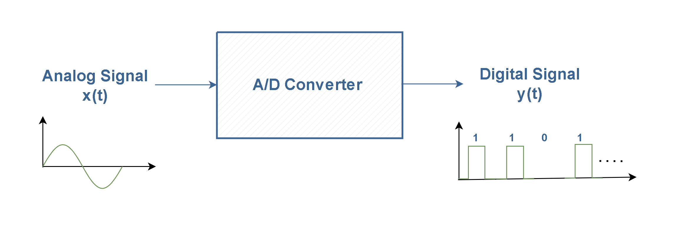
Introduction Author: Aazim Hassan cover photo: depositphotos.com Current loop output sensors are used to transmit data over long distances without dropping the sensor output value. Signal conditioning is performed at the receiving end to analyze and measure the output value.
Introduction
- Author: Aazim Hassan
- cover photo: depositphotos.com
Current loop output sensors are used to transmit data over long distances without dropping the sensor output value. Signal conditioning is performed at the receiving end to analyze and measure the output value. Generally, the output signal is in the range of 4 – 20mA before being conditioned and processed.
This article describes how to use GreenPAK™ for signal conditioning of current loop output sensors. To confirm the sensors are working properly, the GreenPAK design outputs a digital LOW signal when the sensor is disconnected from the system.
This GreenPAK design has an input range of 4 – 20mA and outputs the serial data over the UART Tx line at a 19200 baud rate. The signal can then easily be read on any third-party device on the UART Rx pin.
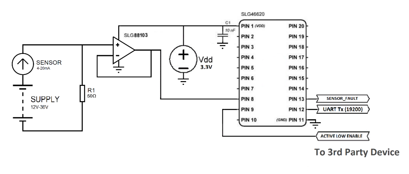
The SLG88103 IC is used as a front-end operational amplifier to convert the current loop signal to analog voltages from 0 – 1V. Next, a SLG46620 is used to convert this analog signal to the RS232 protocol. The SLG46620V is a low-power, cost-effective, small device that can substitute for a system of discrete ICs and passive devices. This unique blend makes the SLG46620 an ideal candidate for portable, cost-sensitive consumer products.
1. Design Overview
Current loop sensors are usually powered through a 12 – 36VDC power source. In this design, the sensor is supplied with a constant DC voltage source in series with a 50Ω resistor. The output current ranges from 4 – 20mA.
We know that by Ohm’s Law, V=IR. At 4mA of current through the 50Ω resistor, the voltage is 0.2V. This is the minimum voltage of the sensor output. At 20mA of current through the 50Ω resistor, the voltage is 1V. This is the maximum voltage of the sensor output.
Whenever the sensor is disconnected from the system, the current through the resistor drops to 0mA and the voltage drops to 0V. We can sense this dropped voltage to detect if the sensor is connected to the system or not.
After conversion, the output from the op amp is fed directly to the SLG46620V at PIN8. Using PGA, ADC, DFFs, and LUTs, the signal through PIN8 is converted to the RS232 protocol, at a configuration of 8 data bits, with 1 even Parity bit at 19200bps. The IC then outputs the data serially on PIN12. To check if the sensor is connected to the system or not, the IC outputs a digital LOW signal at PIN13 whenever the sensor is disconnected from the system.
To make the circuit power efficient, an enable pin (PIN9) disables all the SLG46620V’s macrocells when pulled HIGH, reducing the total power consumption of the IC to less than 10µA. This feature not only decreases the overall current consumption of the system, but also gives control to the third-party device to decide when to process data.
The internal working of the SLG46620V’s macrocells is discussed in detail in the GreenPAK Design section.
2. GreenPAK Design
The design consists of three parts:
- Analog to parallel data conversion
- Parallel to serial data conversion
- Adding Start, Parity and Stop bits
The complete design file can be found here. It was created in free GUI-based GreenPAK Designer software – a part of Go Configure™ Software Hub.
2.1. Analog to Parallel Data Conversion
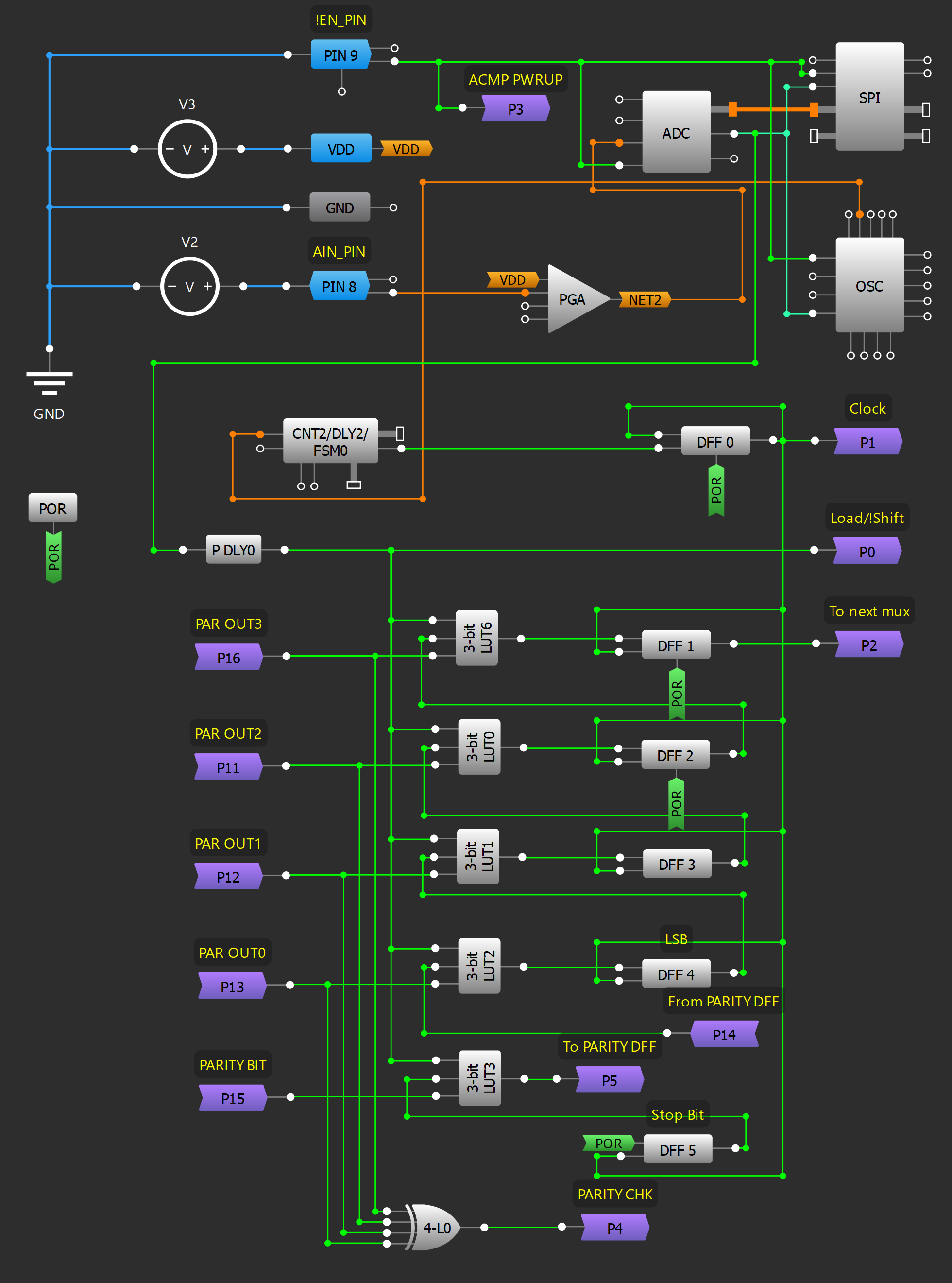
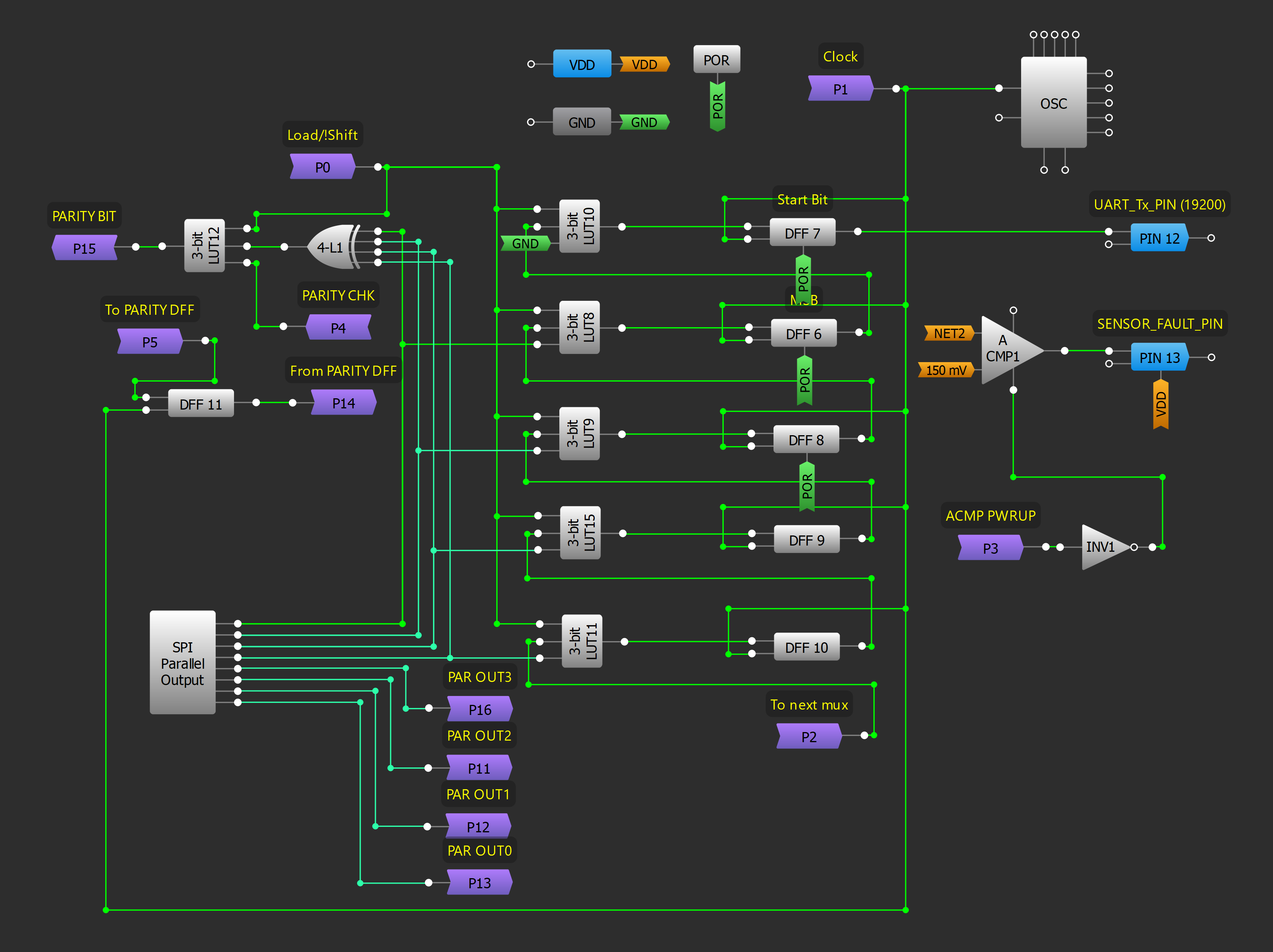
The IC receives the external analog signal through PIN8, which is configured to operate as an analog input/output. The signal then passes through a Programmable Gain Amplifier, or PGA, which sets the gain. Then, the signal enters the analog-to-digital converter (ADC) block. The operation mode of the ADC is single-ended with x1 gain.
The ADC macrocell converts the analog signal in 8 bits of corresponding digital data. This 8-bit digital data from the ADC is fed directly to the SPI macrocell. The configuration of the PGA, ADC, and SPI macrocells can be seen in Figure 2. The SPI macrocell allows parallel data output. By enabling the block in Matrix 1, we can have the data on 8 parallel bits.
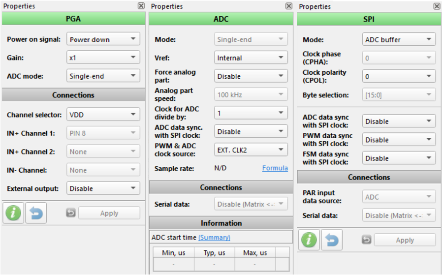
The PWM and ADC clock source is defined as EXT. CLK2, which is the frequency at which our data will be outputted serially from the GreenPAK (19200 bits per second).
The configuration of the OSC macrocell is shown in Figure 3.
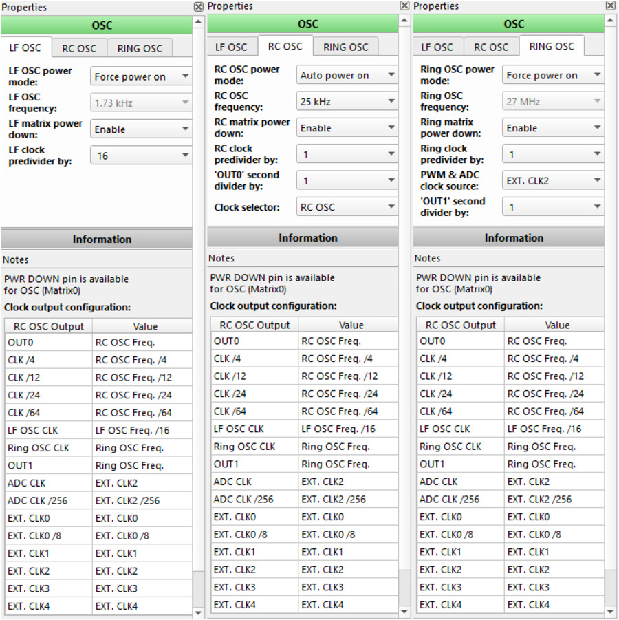
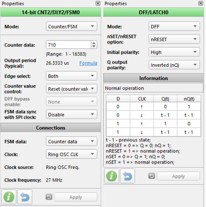
We have generated a clock frequency of 19.2kHz using the 14-bit CNT2/DLY2 and DFF0. This 19.2kHz frequency signal is not only used as the clock source of the ADC, but also to convert parallel data from the parallel data output block to serial data. This is explained further in the next section.
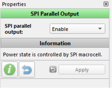
SPI Parallel Output configuration (in Matrix1) is shown in Figure 4.
In the below figure, some wires from Matrix0 are connected to those in Matrix1. GreenPAK Designer has ports to carry signals between matrices. Out-ports from one matrix are available in the other matrix as In-ports, and vice versa.
2.2 Parallel to Serial Conversion
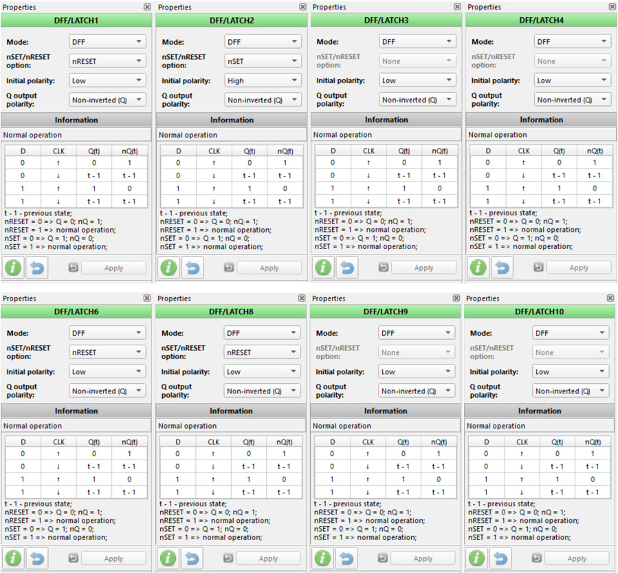
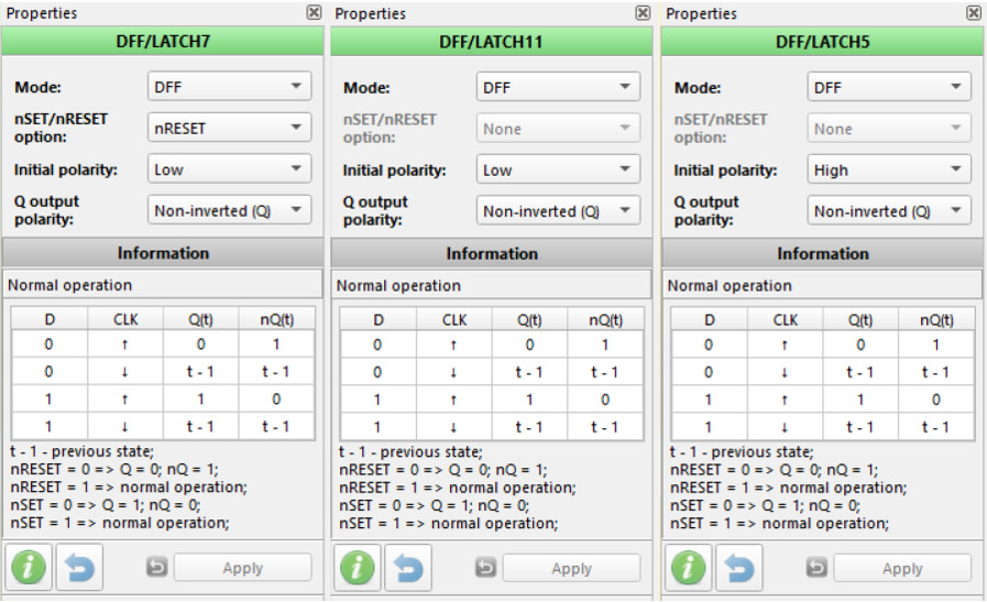
The data from the Parallel Data Output macrocell in Matrix 1 is converted to serial data using a Parallel-In-Serial-Out (PISO) shift register. DFF1, DFF2, DFF3, DFF4 in Matrix0 and DFF6, DFF8, DFF9, DFF10 in Matrix1 are used as 8-bit PISO shift registers to store and transmit data from SPI parallel output serially to PIN12. DFF7, DFF11 and DFF5 are used to add Start, Parity and Stop bits respectively to the serial data. We will discuss these in the next section. Figure 6 shows the configuration of the 8-bit PISO DFFs.
The 8 parallel output bits from the SPI parallel output block are connected with the 8-bit PISO DFFs at the D pin of each DFF. A clock is applied at the CLK pin of the DFFs, which controls the shifting of the bits in the DFFs. Every time a rising edge is inputted at the CLK pin of a DFF, the value (0 or 1) stored in that DFF is shifted to the next DFF. In this way, after 8 consecutive high pulses at the CLK pins, the 8-bit data is outputted from the PISO shift register.
The clock signal at the input of the DFFs is generated using the 14-bit CNT2/DLY2 and DFF0. The frequency of this clock signal is 19200Hz. At this frequency, the GreenPAK communicates at a common baud rate of the RS232 protocol. The most common baud rates are 4800, 9600, 19200, 38400, 57600, and 115200. By selecting the 19200Hz frequency, the data transmit at 19200bps serially through the PISO shift register. The configuration of the 14-bit CNT2/DLY2 and DFF0 are shown in Figure 7.
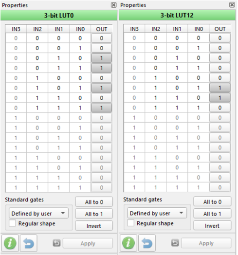
After every successful transmission of the 8-bit data, the next step is to load the next 8 bits of data into the shift register. To do this, we use 3-bit LUTs to form a multiplexer (MUX) design within the SIPO. LUT0, LUT1, LUT2, LUT3, and LUT6 in Matrix0, and LUT8, LUT9, LUT10, LUT11, LUT12, and LUT15 in Matrix1 are used as MUXs.
All these LUTs have exactly the same configuration, except LUT12. Figure 8 shows the configuration of the LUTs.
To load the data within the DFFs, we’ll first look at the timing diagram of the ADC and SPI parallel outputs with respect to the 19200Hz clock frequency as shown in Figure 9.
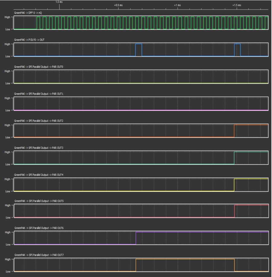
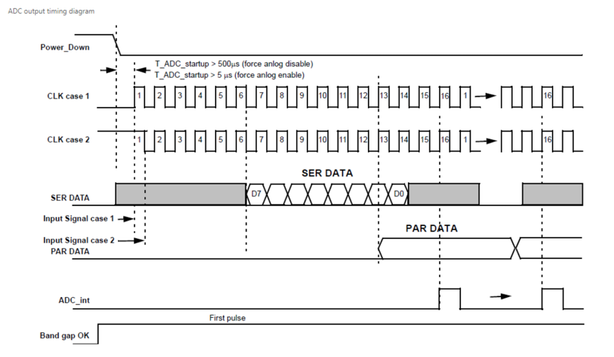
The first waveform in green is the 19200Hz clock signal. The ADC is also supplied with this clock frequency through EXT. CLK2 of the OSC block. The next waveform is the ADC_INT signal of the ADC macrocell. According to GreenPAK Designer, “The Interrupt output is one clock period long and signifies the PAR data is valid.” See the timing diagram of the ADC output in Figure 10.
Using the INT signal from the ADC_INT pin, we will be notified that the data at the parallel bits of the parallel data output is ready to be loaded in the DFFs.
Have a look at the next 8 waveforms carefully. Notice that the states of the outputs are changing with every rising edge of the INT signal. The first signal is PAR OUT0, and it is the least significant bit. The last signal is PAR OUT7, and it is the most significant bit.
By using the multiplexers, we can check for the INT rising edge and load the data into the 8-bit PISO DFFs. The time duration between two consecutive INT pulses is the time we will use to transmit the data serially from the GreenPAK.
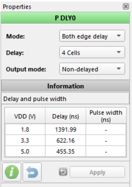
A Programmable Delay (P DLY) logic cell is used to generate a small delay in the signal. We have used this to generate an approximately 500ns delay at the interrupt signal of the ADC to make sure that the data at the parallel output block is available.
2.3 Adding Start, Parity, and Stop Bits
The RS232 protocol communicates 8 data bits in a single packet, with 1 Start bit, 1 Parity bit, and 1 or more Stop bits. After the conversion of our data from an analog signal to parallel data and then to serial data, the last step is to add these bits so that our data becomes standard RS232 data.
DFF7 is used to load the Start bit. The Start bit is one clock pulse long, a digital LOW signal which indicates the start of the data. The next 8 bits after the Start bit are the 8 bits of data.
After the transmission of the Start and 8 data bits, the next bit is a Parity bit. This is either HIGH or LOW depending on the number of 1s in the 8 bits of data. We have a LOW Parity bit if the number of 1s is even and a HIGH Parity bit if the number of 1s is odd. For example, if we have our 8 data bits as 01101000, we have an odd number of 1s and the Parity bit must be HIGH.
To generate a Parity bit, we have used the 4-bit LUT0 in Matrix0, and the 4-bit LUT1 in Matrix1 as XOR gates. An XOR gate has an output HIGH if the number of 1s on the input is odd, and an output LOW if the number of 1s is even. We have inputted these LUTs with the 8 parallel output bits from the SPI parallel output macrocell. At the rising edge of the interrupt signal from the ADC, we check the number of 1s and load the parity bit into DFF11.
A Stop bit is one or more HIGH bits sent after successfully transmitting 1 Start bit, 8 data bits, and 1 Parity bit serially. DFF5 is used to load the Stop bit.
Figure 13 shows the configuration of DFF7, DFF11, and DFF5 for the Start, Parity and Stop bits respectively.
2.4 Sensor Fault Detection
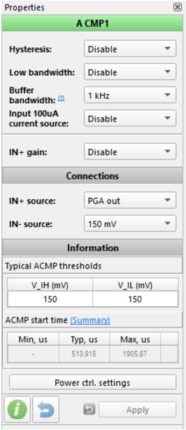
Another interesting feature we can generate using GreenPAK is sensor fault indication. We have used an analog comparator for this purpose, which outputs a digital LOW signal at PIN13 of the GreenPAK SLG46620V whenever the voltage at the input drops below 150mV.
The current loop sensors have a minimum output value of 4mA and a maximum of 20mA. But whenever the sensor is disconnected from the loop, the current drops to 0mA. This results in a signal of 0mV at the AIN_PIN (PIN8 of SLG46620). This signal is fed directly to the third-party device (e.g., Arduino).
ACMP1 in Matrix1 is used as the sensor fault detector. IN+ is set to 150mV, while IN- is supplied with a NET connection from the PGA macrocell.
To enable this feature, we apply the active low enable signal into the inverter INV1 in Matrix1 and connect the output of INV1 to the PWR UP pin of the ACMP1. Figure 14 shows the configuration of ACMP1.
3. Results
The Signal Wizard included in GreenPAK Designer lets us examine the design and ensure it works as expected.
Signal Wizard is very convenient for design inspection, where signals of different shapes can be generated without the need to use an external signal generator. The signal frequency and amplitude can be easily controlled. A custom signal can also be generated.
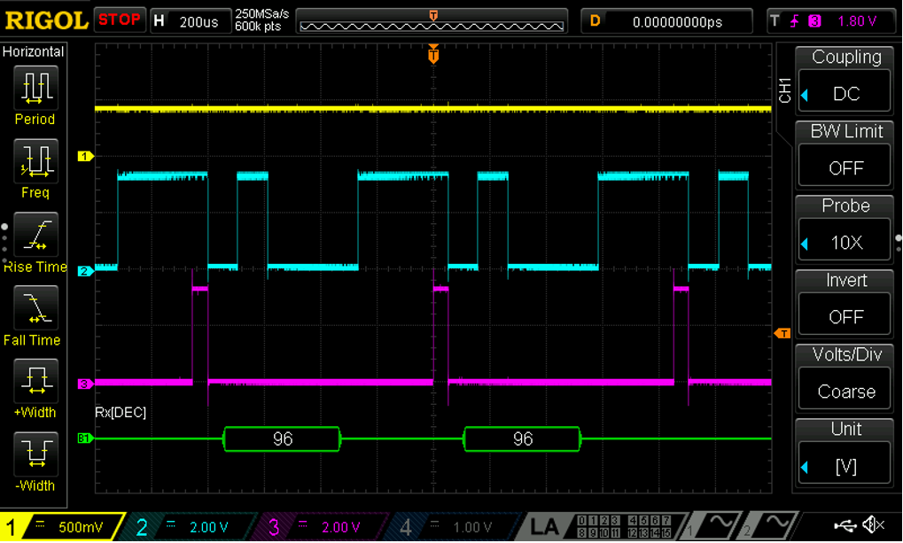
The test results are shown in Figure 15. The second waveform is the input signal applied to the AIN_PIN. Consider the signal at 2.2ms in the signal wizard. It is 300mV. At this position, with the rising edge of the clock signal (last waveform), the UART data is available at PIN12 (third waveform).
Every UART bit starts at the rising edge of the clock signal. The first bit is a LOW signal (0). This indicates the Start bit. The next 8 bits are decoded as 01000101. These are the 8 data bits which carry the actual data.
The bit after the 8 data bits is the Parity bit, which shows the number of 1s in the data. We have a HIGH signal (1) as the Parity bit because the number of 1s are odd in this case.
After the Parity bit, the next 1 or more bits are HIGH Stop bits.
The next data packet starts at the falling edge of UART.
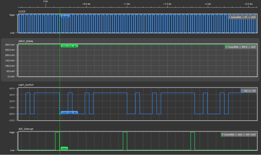
Consider the next UART falling edge at approximately 2.2ms + 0.8ms. The first bit (0) is again a Start bit, followed by the same data bits 01000101, and a Parity bit of 1 since the number of 1s is odd.
4. Arduino Code
Following is the bare minimum code for reading values from GreenPAK on an Arduino development board.
#include <SoftwareSerialParity.h>
SoftwareSerialParity GreenPAK(2, 3); // RX, TX
int i;
void setup()
{
  GreenPAK.begin(19200,EVEN);
  Serial.begin(19200); // start serial to PC
}
void loop()
{
  if (GreenPAK.available() > 0)
  {
  i = GreenPAK.read();
  Serial.print(i, DEC);
  Serial.print(" ");
  }
}
The “Software Serial Parity” library is used to read data with even parity through Arduino. See the References section for more information.
Conclusion
This article outlines how to build a signal conditioning circuit using a GreenPAK, which includes a current loop to RS232 converter circuit at a 19200 baud rate.
The GreenPAK IC demonstrates a high efficiency for integrating several functions in a low-cost and small-area IC solution, making it especially suitable for industrial devices.