Driving down the on resistance of silicon carbide transistors
UnitedSiC has developed silicon carbide transistors in standard packages with the world's lowest on resistance. Chris Dries, CEO, talks to Nick Flaherty about the significance of the move.
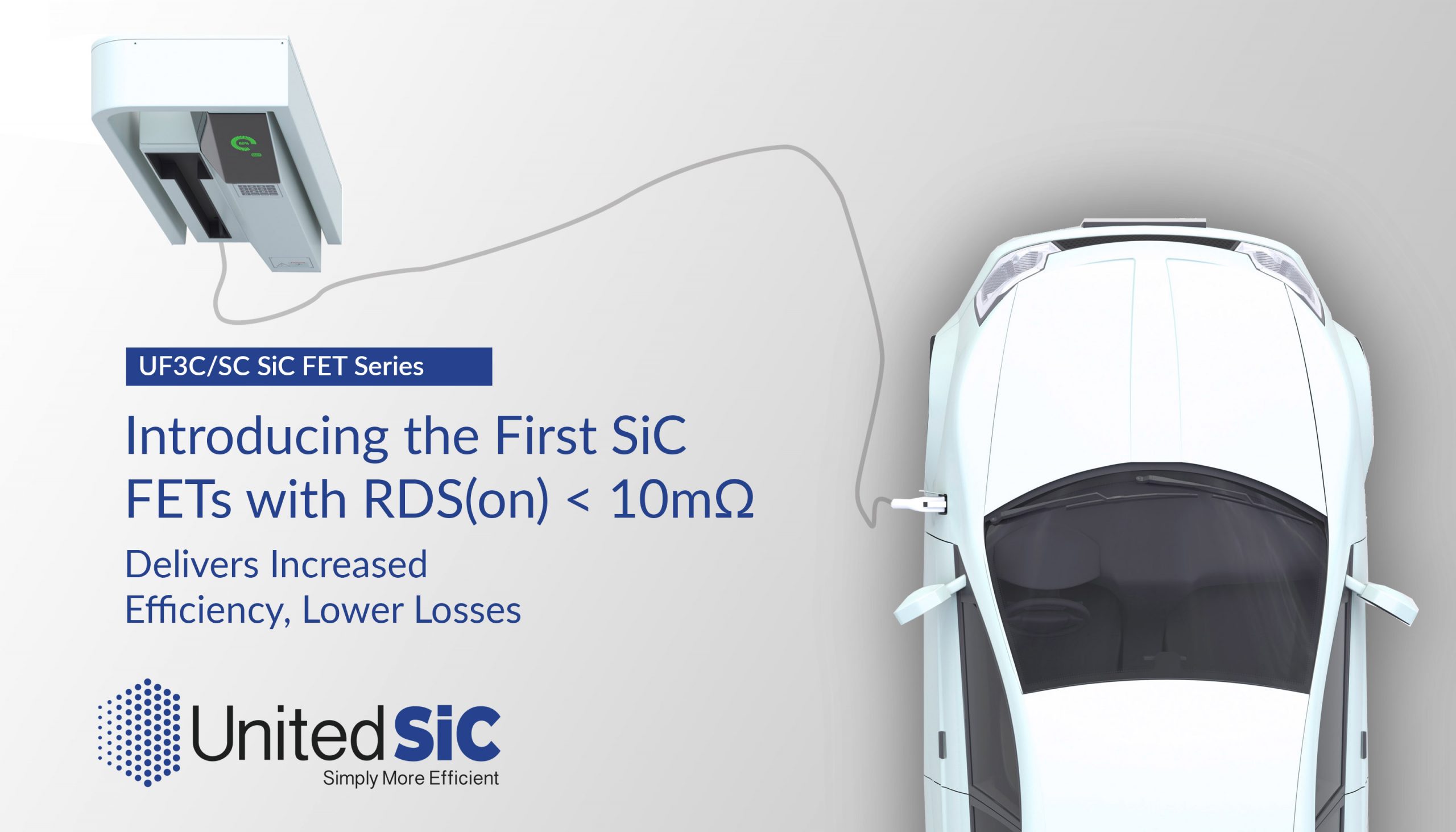
UnitedSiC has launched four silicon carbide SiC transistors with the world’s lowest on resistance RDS(on) to open up new applications.
“What we are doing is pretty incredible for the industry with an on resistance on under 10 mΩ in a standard package,” said Chris Dries, CEO of United SIC, talking to eeNews Power. “This is a real milestone for United SiC. The flagship market for us is electric vehicles, particularly in traction, but circuit protection is a new area now enabled by the low rds on,” he said.
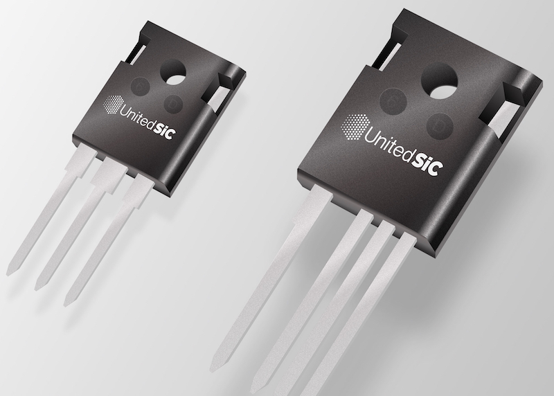
Of the four new SiC FET devices, one is rated at 650V with RDS(on) of 7 mΩ and three rated at 1200V with RDS(on) of 9 and 16 mΩ. These are available in a TO247 package with three or four pins.
“This is an extension of the third generation platform – the maturation of the process in the fab enables us to go to these large die at high volume” said Dries. “We have created two different types of FET depending on the switching speeds – the UJ3C is general purpose that is easy as a drop in replacement, while the UF fast parts are designed for high performance hard switched.”
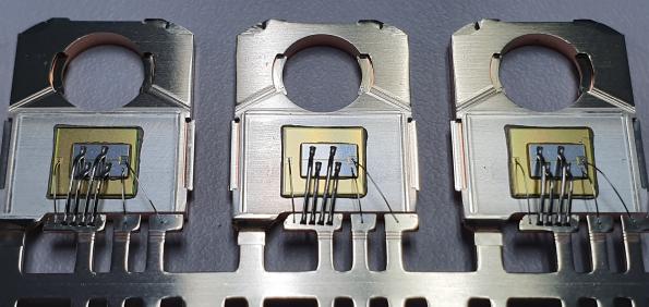
This comes from the design of the parts, which uses a silicon MOSFET, or cascode, alongside a JFET built in silicon carbide.
“The silicon cascode MOSFET that we make is stacked on top of the JFET,” he said. “The way we are able to do it is because the underlying technology of the JFET – RDS(on) per unit area – at 1200V our specific on resistance is half at 1200V and at 650V is a quarter. That’s the key differentiator that allow us to do this where other cannot.”
“The problem with SiC is that it does not like to form a gate oxide,” said Dries. “What we have done is use the perfect oxide of silicon as the gate interface and then we have the SiC JFET with the lowest specific rds on, so we optimise the performance of both FETs. Its really hard to do it successfully but once you can it’s the best way,” he added.
While the 4pin versions are aimed at high frequency switching, the three pin versions are drop in replacements for silicon IGBTs.
“The 3pin version is to directly replace CoolMOS [devices from Infineon] in low RDS on designs. Designers can move from 2.2, 2.4kW to 3kW by replacing CoolMOS silicon with drop in SiC. Most SiC MOSFETs need a negative gate drive from -4 or -5V to +15 or 20V, but we design the gates so they are clamped at -20V so we can be pin for pin compatible with silicon IGBTs.”
Thermal management is a key part of the new devices. “What we do is silver sinter the die to the lead frame using die attach technology that allows us to get the heat out of the package. We can do a three lead (3L) package but the di/dt necessitates a four pin kelvin connected package,” he said. “In the SiC industry we all have this four lead package – Infineon, Cree, ST all have it – the switching performance is far superior and we try to steer customers to it. Those parts can run at over 100A in a TO247 package.”
The low conduction losses mean the devices can also be used as solid-state circuit breakers and battery disconnect switches in electric vehicles. The devices can turn off very high currents very quickly, and when used as a circuit breaker have a self-limiting characteristic that controls the peak current that flows. This characteristic can also be used to limit inrush currents flowing into inverters and motors.
“Solid state circuit breakers s a new and emerging market for us, enabled by the low RDS on devices. Initial customers tend to be in the aerospace industry to route power in an aircraft,” said Dries. “When paralleled can surge rating over 100A and turn off safely. With six die in parallel you get a 2 mΩ switch in a SOT227 1200V module.”
The UF3SC065007K4S has a maximum operating voltage of 650V, a drain current of up to 120A, and an RDS(ON) of 6.7mΩ. The UF3SC120009K4S has a maximum operating voltage of 1200V, drain current of up to 120A, and an RDS(on) of 8.6mΩ. Both come in a four-lead Kelvin package, enabling cleaner drive characteristics.
For lower-power designs, UnitedSiC offers two parts with maximum operating voltages of 1200V, drain currents of up to 77A, and an RDS(on) of 16mΩ. The UF3SC120016K3S has a three-lead package, while the UF3SC120016K4S has a four-lead package.
The parts are built at X-Fab’s foundry in Texas using the IP and process technology from United SiC, with a capacity of 30,000 wafers a month, says Dries. The company uses three suppliers of SiC wafers.
“We have three qualified suppliers of substrates and we see no differentiation in quality for yield based on the substrate or epi for the JFETs, and we run equivalent yield s on all three suppliers,” said Dries. “Historically its important in a new material system to own the material supply but over time that becomes commoditised. That’s what happened in gallium arsenide (GaAs) and indium phosphate (InP) and I think the same thing will happen over time,” he said.
more information: www.unitedsic.com
article is re-published from www.eenewspower.com and written by Nick Flaherty.


The car is so interested,how long does it go for it to charge again?