


“NanoEngineers” research group at Iowa University have been devoting efforts to use graphene and its amazing properties in their sensors and other technologies. Graphene has many extraordinary properties. It is about 100 times stronger than the strongest steel. It conducts heat and electricity efficiently and is nearly transparent.
Inspired by some recent projects about using inkjet printers to print multi-layer graphene circuits and electrodes, “NanoEngineers” have been working to move this research further by using the technology for a larger scale flexible, wearable and low-cost electronics. But there was some hurdles in improving the graphene conductivity after being printed and this process may damage the printing surface, such as papers, because of the high temperature or the use of chemicals.
Eventually, these engineers have led development of a laser-treatment process that allows them to use and improve printed graphene for electronic circuits and electrodes, even on paper and other fragile surfaces. The technology is said to show tremendous promise for a wide variety of fields including wearable sensors and thin film transistors with the ability of large-scale manufacturing.
It’s a three step process:
- Graphene ink formulation: single layer graphene (SLG) powders were mixed with solvents and binders, bath sonicated, probe sonicated, and syringe filtered in order to produce a jettable graphene ink.
- Inkjet Printing: The resultant graphene ink was syringed into the printer cartridge of a Dimatix Materials Printer and ejected via a piezoelectric nozzle in the subsequent printing process.
- Laser Annealing: A pulsed-laser processing of the electrodes using a Nd:Yag laser.
The engineers were able to remove ink binders and reduce graphene oxide by developing a computer-controlled laser technology that selectively irradiates inkjet-printed graphene oxide, Transforming the inkjet-printed graphene into a conductive material capable of being used in new applications is a huge breakthrough in nanotechnology.
More details are available at this paper on NanoScale journal.
Via: ScienceDaily
RELATED POSTS
 30 April, 2020 Arduino-Based SSD uses an ATmega8 & 8 EEPROM chips
 7 May, 2018 Solid State Li-ion Batteries – High Energy-Dense Batteries Are Closer Than Before
 25 September, 2023 Industrial mini PC from ICOP Features Modern OS Support, Wide Temperature Range and Support for Various I/O Interfaces
 2 January, 2018 XMotion All In One Controller for Robotics
 30 July, 2022 The new UP 4000 aims to Bridge the Gap to the Next Generation UP Board
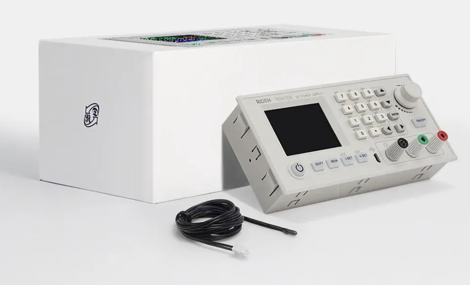 17 August, 2020 RD6006 Digital Control Switch Adjustable Power Supply starts from just $57