Create +/-12V Split Rail From A 5V Bias
With digital semiconductor technology driving system power supplies to lower voltages for higher performance and lower system power, sensitive analog sensor circuits face a growing problem. Much of the inherent noise created in the early stages of an analog sensor signal path is independent of the amplifier bias voltage, so using a higher bias voltage yields better accuracy and performance than a lower bias.
With digital semiconductor technology driving system power supplies to lower voltages for higher performance and lower system power, sensitive analog sensor circuits face a growing problem. Much of the inherent noise created in the early stages of an analog sensor signal path is independent of the amplifier bias voltage, so using a higher bias voltage yields better accuracy and performance than a lower bias. With supply voltages dropping, then, designers must tolerate the loss of accuracy (SNR) due to the lower available voltage or derive a higher voltage bias from the available system supply.
In addition to the voltage, designers need to consider the ground. In many cases the sensor circuit must have bias voltages both above and below signal ground. That signal ground can be either a true system ground or a virtual ground created at the midpoint of a single-rail power supply. Using a true system ground requires “split-rail” biasing (±V), but yields improved performance as a result of reduced leakage currents and reduced variations in a virtual ground, both of which affect measurement accuracy.
to help improve the performance and signal-to-noise ratio of analog sensor front ends.
To obtain the best performance from the analog front end, then, designers need a method of creating a higher voltage split-rail bias from a lower-voltage single-rail supply. One way to create this split-rail voltage is to use a switch-mode regulator IC in concert with a small transformer. This forms a flyback design that uses less than one square inch of board space.
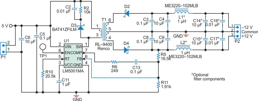
The circuit of Figure 1 boosts a nominal 5-V single-rail supply (4.5 to 5.5 V) to a low-noise, ±12-V bias and can be adapted to develop other voltages such as ±15 V. The design uses a Texas Instruments LM5001 (U1) switch-mode regulator that integrates a pulse-width modulation (PWM) generator, a switching transistor, a voltage reference, and an error amplifier that controls the PWM duty cycle based on a comparison between the reference and the feedback signal on pin 6.
The regulator switches current through the primary of center-tapped transformer T1, and the PWM duty cycle determines the output voltage at the secondary. Diode D3 and its attached components serve as a snubber to minimize transient noise and ringing on the transformer input when the regulator’s internal switch opens. Diodes D2 and D4 serve as half-wave rectifiers for the transformer’s output.
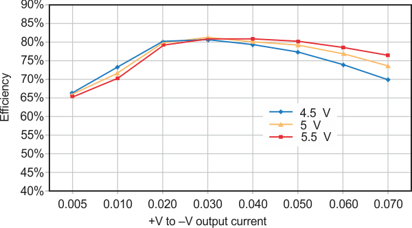
but conversion efficiencies greater than 80% are attainable.
Resistor R10 sets the PWM’s nominal switching frequency to 600 kHz, which represents a compromise between conversion efficiency and noise (both switching noise and ripple) on the bias voltage outputs and transformer size. With this frequency, conversion efficiency (Fig. 2) can be greater than 80% depending on load. Both noise and conversion efficiency decrease with increasing switching frequency, so designers can choose to increase efficiency at the expense of noise by adjusting the value of R10. Decreasing the switching frequency often results in the need to increase the size of the transformer, adding to this tradeoff decision.
Capacitors C3, C4, C8, and C9 serve as the principal output filters, but designers can further reduce switching noise by incorporating the optional low-pass post filters L1/C14 and L2/C15 shown on the positive and negative outputs. The filters have a cutoff frequency of about 90 kHz, resulting in less than 10-mV peak-to-peak transient noise and under 2-mV switching ripple measured from dc to 600 MHz. Designers can reduce this noise even further by changing C4 and C9 to 47 µF. Symmetrical layout of the design’s differential power section can help reduce differential noise.
This type of flyback design, which uses only one regulator monitoring the positive output, provides common-mode rejection of some noise components and only uses a single IC. Cross regulation is typically not as tight with one regulator as would be possible when using a separate regulator for the negative output. But since most sensor signal path circuits draw symmetrical current on each rail, cross regulation usually isn’t an issue.
In any case, measurements show good cross regulation with this circuit. Either output maintains regulation to less than 3% when delivering 35 mA while the other output load varies between 10 mA and 50 mA. The design’s measured output tolerance is within 5 mV across both outputs when delivering from 5 to 40 mA from both outputs differentially.


