Understanding Flash Memory And How It Works
Flash memory is one of the most widely used types of non-volatile memory. NAND Flash is designed for modern file storage which replaced old disk drives.
Flash memory is one of the most widely used types of non-volatile memory. NAND Flash is designed for modern file storage which replaced old disk drives. This article provides a brief understanding of how NAND Flash technology works.
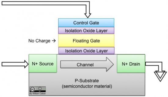
The basic storage component used in Flash memory is a modified transistor. In a standard transistor, the flow of current through a channel between two contacts is turned on by a voltage applied to the gate. The channels are separated by an insulating layer of Oxide. In a Flash storage cell, there is an extra electrically isolated gate called “floating gate”. It is added to the control gate and the channel of the modified transistor.

High voltage is applied to the control gate of The Flash cell to program it. This pushes electrons to pass through the oxide layer to the floating gate (a process known as tunneling). The presence of these trapped electrons on the floating gate changes the required voltage to turn on the transistor. Thus, a transistor with no charge on the floating gate can easily turn on at a certain voltage, representing a 1, while a programmed cell will not turn on, representing a 0.
This kind of memory is non-volatile because the floating gate is surrounded by dielectric layers, it traps the electric charge even when the power is removed. Erasing a cell reverses this process by introducing a large negative voltage to the control gate to force the electrons to tunnel out of the floating gate.
A number of cells, typically 32 to 128, are connected in a string. Strings are organized in blocks. To program cells in a block, the data is put on the bit lines and a high voltage is applied. Because programming can only change a cell from a 1 to a 0, any cells where the new data is a 1, will be left in their current state. Therefore, all the cells must be erased before writing. This process ensures that any cells that will not be programmed already contain a 1.
As explained above, each cell can store a single binary value, 0 or 1. It is also possible to inject varying amounts of charge onto the floating gate so that the cell can express multiple values. A multi-level cell (MLC) can store four different levels to represent two bits. However, the performance is reduced because of the complexity of accurate voltage controls. For the same reason, MLC Flash memory is more inclined to errors.
Although flash memory has a limited number of write-erase cycles, the high voltages cause a small amount of damage to the cells which makes them harder to read-write over time. The main drawback of using a flash memory is that it has a lifetime of about 100,000 cycles or fewer for MLC Flash.


